Signal Integrity Design for Gigabit Device PCB board
It introduces the application of PCB board design tools to solve these problems, such as skin effect and dielectric loss, the effect of vias and connectors.
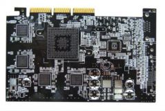
PCB board layout design review elements
The preferred process route has been determined, and all devices have been placed on the PCB board.