Blog

e539eabb03275ea0236b22515c7f3044_250x160
Experience Summary of Mobile Phone RF circuit board Layout and Wiring
be07c050b2985d846da46501e2651c25_250x160
Prevention and leveling method of PCB board warpage
People in the industry are well aware of the impact of PCB board? warpage.
a6de8b86f4c56e9c4c052db5ddd0fcf2_250x160
How is a good PCB board made
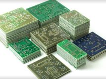
Everyone knows that making a PCB board is to turn a designed schematic into a real printed circuit b...
2f2096792f73db99b92c38e7b5350ff5_250x160
The difference between analog circuits and digital circuits in PCB board design
1394dbd9f1591b9b0fe83aba0d87dc14_250x160
High-quality PCB board design should pay attention to inventory
?Reasonable arrangement of components is the basic premise of designing a high-quality PCB board? la...
07916f85d07ae62b90eb5e4388f1d632_250x160
Some good PCB board routing skills and essentials
In the PCB board? design process wiring is a skill that is limited and limited.
03a639495061c4a4cd1584697acfc1d6_250x160
Detail the basic rules of PCB layout and wiring
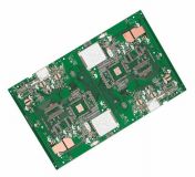
?PCB, also known as Printed Circuit Boards?, can realize circuit connection and function realization...
5f6fa3ad8eb78424304a4892dc18f80a_250x160
The role of layered stacking of PCB boards in controlling EMI radiation
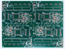
This article starts from basic PCB board layout and discusses the role and design techniques of layered...
56c129598c246e4556b8e9c6a24714b5_250x160
High frequency PCB board wiring rules
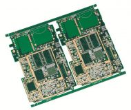
Under normal conditions, all components should be arranged on the same side of the printed circuit b...
b2f0cb9582d8cca528d4886e0f1911e9_250x160
PCB board design principles to reduce electromagnetic interference
The effective anti-interference design of the PCB board? is a key link in the design of electronic products,...
1 62 63 64 65 66 68

Are You Ready to Start Getting Your Quote?

Free, Fast, and Secure.