Skip to content
HOME
PCB MANUFACTURING
PCB Prototype
Aluminum PCB
Double-Sided PCB
Flex PCB
HDI PCB
High-frequency PCB
Multilayer PCB
Rigid PCB
Rigid-Flex PCB
Rogers PCB
Single Layer PCB
Teflon PCB
PCB Assembly
Fast Prototype PCB Assembly
SMT PCB Assembly
Through-hole PCB Assembly
Quick Turn PCB Assembly Services
PCB SMT Solder paste Stencils
Low-Cost PCB Assembly Service
Low Volume PCB Assembly
LED PCB Assembly
Lead-free PCB Assembly Service
Full & Partial Turnkey PCB Assembly
Components Purchasing Services
COMPONENTS
CATEGORIES
Manufactuers
ELECTRODESIGN
RESOURCES
Support
Flying Probe Testing for PCB
X-ray Inspection in PCB Assembly
PCB & PCBA Manufacturing File
IPC Class
What is the BOM?
FAQ
Blog
PCB Blog
PCB News
IC Substrate
Electronic Design
PCBA Tech
Microwave Tech
About Us
Contact Us
X
sales@ptpcba.com
Category: PCB Blog
首页
PCB Blog
Page 47
PCB Blog
Electronic Design
IC Substrate
Microwave Tech
PCB News
PCBA Tech
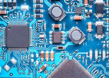
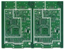
New UV laser processing technology for PCB board and substrate
New UV laser processing technology for PCB board? and substrate.
June 24, 2022
Read More
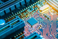
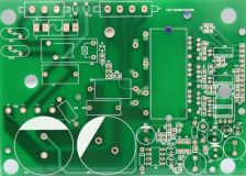
Six types of module PCB board debugging technology
The components of the six types of modules are PCB board.
June 24, 2022
Read More
Analysis of PCB board electrical measurement technology
In the production process of PCB board, it is inevitable that electrical defects such as short circuits,...
June 23, 2022
Read More
Design Method of High Speed Digital PCB Board for Signal Integrity
This paper introduces a design method for a high-speed digital signal PCB board based on computer analysis...
June 23, 2022
Read More
The Role of PCB Board Layer Stacking in Controlling EMI Radiation
This article starts with a basic PCB board layout and discusses the role and design techniques of PCB...
June 22, 2022
Read More
Basic concepts of PCB board design
Due to special requirements such as anti-interference and wiring, the PCB board used in some newer electronic...
June 21, 2022
Read More
Methods of Anti-Electrostatic Discharge (ESD) when designing PCB board
?In the design of the PCB board, the anti-ESD design of the PCB board can be realized by layering, proper...
June 20, 2022
Read More
Wet process and PCB Board surface treatment
The wet spray pumice powder (Pumice) technology that has been used in the PCB board? manufacturing process...
June 20, 2022
Read More
PCB board design technology in SMT environment in detail
The SMT process uses solder or solder paste to form a mechanical and electrical connection between the...
June 17, 2022
Read More
Methods to Reduce RF Effects in PCB Board Interconnect Design
The interconnection of PCB board? system includes a chip to the circuit board, interconnection within...
June 17, 2022
Read More
No posts found
Posts pagination
1
…
46
47
48
…
68
86-755-27808737
sales@ptpcba.com
We will reply within 24 hours.
Business
Cooperation
Others
Phone
Email
Submit
Cancel
8614704450345