Skip to content
HOME
PCB MANUFACTURING
PCB Prototype
Aluminum PCB
Double-Sided PCB
Flex PCB
HDI PCB
High-frequency PCB
Multilayer PCB
Rigid PCB
Rigid-Flex PCB
Rogers PCB
Single Layer PCB
Teflon PCB
PCB Assembly
Fast Prototype PCB Assembly
SMT PCB Assembly
Through-hole PCB Assembly
Quick Turn PCB Assembly Services
PCB SMT Solder paste Stencils
Low-Cost PCB Assembly Service
Low Volume PCB Assembly
LED PCB Assembly
Lead-free PCB Assembly Service
Full & Partial Turnkey PCB Assembly
Components Purchasing Services
COMPONENTS
CATEGORIES
Manufactuers
ELECTRODESIGN
RESOURCES
Support
Flying Probe Testing for PCB
X-ray Inspection in PCB Assembly
PCB & PCBA Manufacturing File
IPC Class
What is the BOM?
FAQ
Blog
PCB Blog
PCB News
IC Substrate
Electronic Design
PCBA Tech
Microwave Tech
About Us
X
sales@ptpcba.com
Category: PCB Blog
首页
PCB Blog
Page 52
PCB Blog
Electronic Design
IC Substrate
Microwave Tech
PCB News
PCBA Tech
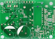
Functional segmentation of high-speed PCB board
Most PCB boards contain some functional subsystems or areas, each functional subsystem consists of a...
May 9, 2022
Read More
Termination of high-speed PCB board
In a high-speed PCB board? system, the impedance mismatch on the transmission line will cause signal...
May 6, 2022
Read More
Noise on PCB board circuit
For the noise on the PCB board, when it is found that electromagnetic interference occurs in the digital...
May 6, 2022
Read More
Radiation from PCB board
The main purpose of the electromagnetic compatibility design of the PCB board is to reduce the electromagnetic...
May 5, 2022
Read More
Examples of PCB board wiring techniques
The design of the mixed-signal circuit PCB board is very complicated.
May 5, 2022
Read More
Introduction and Troubleshooting of Nickel Electroplating on PCB board
?Nickel plating is used on PCB board as a substrate coating for precious metals and base metals, and...
April 29, 2022
Read More
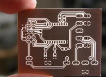
The operation process of PCB board photopainting (CAM)
About the operation process of PCB board light painting.
April 29, 2022
Read More
How to prevent ESD when designing PCB board
Use multi-layer PCB board as much as possible.
April 28, 2022
Read More
Reflection caused by changes in PCB board trace width
When conducting PCB board wiring, it often happens that when the traces pass through a certain area.
April 28, 2022
Read More
The solution of PCB board mounting SMD on FPC
The solution of PCB board mounting SMD on FPC,According to the placement accuracy requirements and the...
April 27, 2022
Read More
No posts found
Posts pagination
1
…
51
52
53
…
68