Skip to content
HOME
PCB MANUFACTURING
PCB Prototype
Aluminum PCB
Double-Sided PCB
Flex PCB
HDI PCB
High-frequency PCB
Multilayer PCB
Rigid PCB
Rigid-Flex PCB
Rogers PCB
Single Layer PCB
Teflon PCB
PCB Assembly
Fast Prototype PCB Assembly
SMT PCB Assembly
Through-hole PCB Assembly
Quick Turn PCB Assembly Services
PCB SMT Solder paste Stencils
Low-Cost PCB Assembly Service
Low Volume PCB Assembly
LED PCB Assembly
Lead-free PCB Assembly Service
Full & Partial Turnkey PCB Assembly
Components Purchasing Services
COMPONENTS
CATEGORIES
Manufactuers
ELECTRODESIGN
RESOURCES
Support
Flying Probe Testing for PCB
X-ray Inspection in PCB Assembly
PCB & PCBA Manufacturing File
IPC Class
What is the BOM?
FAQ
Blog
PCB Blog
PCB News
IC Substrate
Electronic Design
PCBA Tech
Microwave Tech
About Us
X
sales@ptpcba.com
Category: PCB Blog
首页
PCB Blog
Page 63
PCB Blog
Electronic Design
IC Substrate
Microwave Tech
PCB News
PCBA Tech
Wearable PCB Board Design Requires Focus on Basic Materials
Due to their small size and size, there are few ready-made printed circuit boards ?standards for the...
February 9, 2022
Read More
Selection skills of magnetic beads in PCB circuit design
In PCB board design the reason for using SMD magnetic beads and SMD inductors: whether to use SMD magnetic...
February 9, 2022
Read More
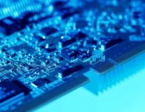
Etching process and process control of printed circuit board
The process of printed circuit board from optical board to displaying circuit pattern is a complex process...
January 23, 2022
Read More
HASL hot air solder leveling process for PCB
HASL is a relatively mature technology at present, but its quality is difficult to control and stabilize...
January 23, 2022
Read More
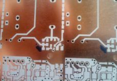
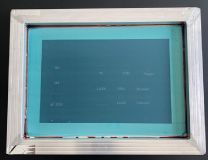
PCB Screen Printing Board Manufacturing Process
PCB Screen Printing Board Manufacturing Process, PCB Bandage Steps: Frame Cleaning--Horizontal Verification--Layered...
January 23, 2022
Read More
EMI Control Technology in Digital Circuit PCB Design
EMI in printed circuit boards? design is caused by sources of electromagnetic interference that transfer...
January 21, 2022
Read More
Talking about how to make a PCB board from five aspects
Everyone knows that making a PCB board? is to turn a designed schematic into a real PCB board.
January 21, 2022
Read More
Three special routing techniques in PCB board design and wiring
The quality of PCB board? design and wiring will directly affect the performance of the entire system,...
January 20, 2022
Read More
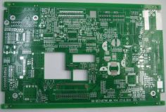
PCB board stackup design
There are many factors that need to be considered to determine the laminated structure of the multilayer...
January 20, 2022
Read More
Experience Summary of Mobile Phone RF circuit board Layout and Wiring
Experience Summary of Mobile Phone RF circuit board Layout and Wiring
January 19, 2022
Read More
No posts found
Posts pagination
1
…
62
63
64
…
68